![]()
Please 'Boom' Responsibly As most of you have noticed, the noise ordinances have become much tougher lately. Most of this is due to idiots, yes IDIOTS, who drive through residential areas with their windows down while their system is playing at full power. To make things worse, the music they listen to has all sorts of foul language that's not suitable for small children, (who may be playing outside). There are even a few people, who are even beyond idiot status, that play their systems at full power through residential areas after 10:00 PM (when many people go to bed). I don't believe that this type of behavior is good for the industry. If the fines get too stiff, people will stop buying large systems. If this happens, more people will get out of car audio (who wants a mediocre system). People get interested in things because they're exciting. A deck and four 6.5" speakers are not going to interest many of the younger car audio enthusiasts. If car audio enthusiasts keep annoying more and more people, the fines will keep getting tougher. All of this will only reduce interest in the equipment that fuels the industry. If you want to listen to your system at full volume, get out on the highway where there's little chance of bothering anyone. When you get to a red light, turn it down. If the only thing attractive about you is your 'system', you have some work to do. Bottom line... Think about what you're doing. Think about other people. It's not the end of the world if you have to turn the volume down for a little while. |
| Factors
which accelerate transistor failure, and therefore
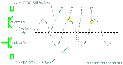
amplifier failure Amplifier Failure: One of the main reasons that amplifiers fail is improper speaker connection. If too many speakers are connected to an amplifier, the amplifier will be more likely to fail. This section will help you to understand why too many speakers will cause an amplifier to fail. Output Basics: The diagram below shows a few parts of an amplifier. You will notice that the amplifier has a power supply which produces output voltages of (+)35 volts DC and (-)35 volts DC. The +35 volts is the supply voltage for the PNP bipolar transistor labeled 'transistor A'. Anytime that the output voltage of the amplifier (to the speaker) is a positive voltage, the PNP transistor will allow the proper amount of current to flow from the +35v supply. When the output voltage is negative, the NPN transistor will allow the proper amount of current to flow from the -35v supply.
The voltage at all points along the sine wave are the instantaneous voltages applied to the speaker. When you come across the power dissipation figures, keep in mind that 35 watts is enough power dissipation to keep a soldering iron at more than 700 degrees fahrenheit. Output Voltage at Point "A": At point A, the output voltage is 0 volts. The speaker would be at its point of rest. There would be no current flowing through the output transistors (except a small amount of bias current). There is virtually no power dissipation at this point. In the following calculations: Psp is the power dissipation in the speaker's voice coil. Ptr is the power dissipation in the transistor. Psp = E²/R Psp = 0²/4 Psp = 0 watts Ptr = I*E Ptr = 0*35 Ptr = 0 watts Output Voltage at Point "B" At point B, the output voltage of the amplifier is essentially the same as the supply voltage. The voltage across the PNP transistor is approximately 0 volts (it is fully turned on). The current flowing through the PNP transistor is as high as it can be with the current speaker load (lets assume that it is a 4 ohm speaker). Since we know that we have a 4 ohm speaker and 35 volts applied to it, we know (for this point in time): the current passing through the PNP transistor to the speaker is 8.75 amps (I=E/R). There is virtually no power dissipation across the PNP transistor. There is no current flowing through the NPN transistor. If you could take a 'snap shot' of the speaker at this point in time, the speaker would be pushed OUT as far out as the amplifier is able. Itotal = V/R Itotal = 35/4 Itotal = 8.75 amps Psp = E²/R Psp = 35²/4 Psp = ~306 watts Ptr = I*E Ptr = 8.75*0 Ptr = 0 watts If the speaker load is 2 ohms, the current flowing through the PNP transistor would double to 17.5 amps. The power dissipation in the PNP transistor would not increase significantly because the voltage across it is very small. Output Voltage at Point "C" At point C, the output voltage of the amplifier is below the reference which means that the voltage is negative (with respect to the reference). The output voltage is approximately -15 volts. This means that the voltage across the NPN transistor is 20 volts (the supply voltage - the output voltage). The current through the speaker AND the NPN transistor is 3.75 amps. The power dissipation in the speaker is 56.25 watts (P=I*E). The power dissipation in the transistor is 75 watts. There is no current flowing in the PNP transistor. A snap shot of the speaker at this point would show the speaker pulled IN approximately 1/2 as far as the amplifier is able. Itotal = V/R Itotal = 15/4 Itotal = 3.75 amps Psp = I*E Psp = 3.75*15 Psp = 56.25 watts Ptr = I*E Ptr = 3.75*20 Ptr = 75 watts A 2 ohm load would result in 150 watts being dissipated in the NPN transistor (twice the power caused by the 4 ohm load). Output Voltage at Point "D" At point D, The output voltage of the amplifier is approximately +20 volts. This means that the voltage across the PNP transistor is 15 volts. We know that 20 volts is applied to the 4 ohm speaker. This means that the current through the speaker AND the PNP transistor is 5 amps. This tells us that the power dissipation across the speaker is 100 watts. The PNP transistor is dissipating 75 watts. There is no current flowing through the NPN transistor. Itotal = V/R Itotal = 20/4 Itotal = 5 amps Psp = I*E Psp = 5*20 Psp = 100 watts Ptr = I*E Ptr = 5*15 Ptr = 75 watts A 2 ohm speaker load would cause the current to double to 10 amps. Since the PNP transistor has 15 volts across it, the power dissipation would be 150 watts. From this and earlier pages, you should remember:
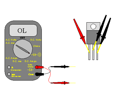
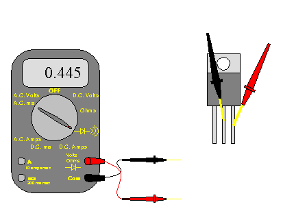
From the above statements, you should be able to see that bridging an amplifier into a load with a lower impedance than recommended will very quickly push an amplifiers components past their design limits. Checking Field Effect Transistors The following diagrams will show you how to check an FET to see if it is bad. This is only for N channel enhancement mode FETs (the type used in most amplifiers' power supplies). Since I use Fluke meters exclusively, all measurements will show what you would see with a Fluke meter. Other digital meters should give very similar readings. Until you become extremely familiar with FETs, you should check the FET in this order from top to bottom. If the order is changed, you may not get accurate test results. This image is checking to see if the gate is leaking or shorted. In this type of FET, the gate should be COMPLETELY isolated from the other two terminals when checking the transistor with a volt meter. During this first test, you are inadvertently charging the gate and turning the transistor on. Sometimes you can even hear it say oooohhh yeah... do that again. :-) The meter should read the same as if the leads are open (not touching anything). You should notice that there are two black leads. this means that you first check the transistor with the red lead on the first leg and the black lead on the second leg. Then you move the black lead to the third leg of the transistor (while leaving the red lead on the first leg). The readings should be the same in both positions. The meter is set to its 'diode check' position.
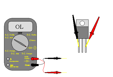
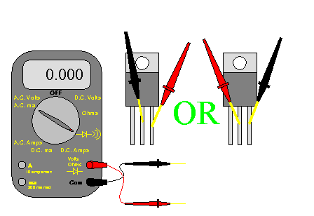
In this image, you are discharging the gate and making sure that the transistor is turned off for the next test. The meter should again read the same as if the leads are open (not touching anything). If it gives any other reading, the transistor is bad.
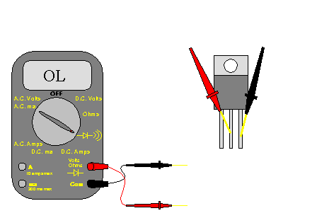
In this image, you're checking to see if there is any leakage between the drain and the source. The meter should again show no continuity between the drain and the source.
In this image, your meter should read approximately 0.4 to 0.5 volts on diode check (the same meter setting as the previous tests). Here the meter is showing the forward voltage of the intrinsic diode of the FET.
If you get any reading other than 'open' on the first 3 tests, the transistor is defective. If the readings on the last test is below approximately 0.4 volts, the transistor is likely defective. If it reads around 0.3 volts or lower, the FET is definitely defective. The transistor is bad in both of these examples. It shows that the drain and source are shorted together.
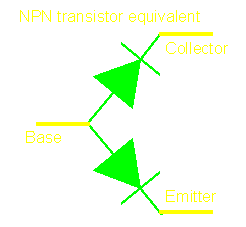
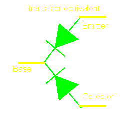
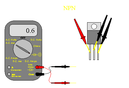
Checking Bipolar Junction Transistors This type of transistor is used throughout all types of electronic equipment. To check PNP transistors, reverse the positions of the red and black leads. This is a close approximation of the junctions in both NPN and PNP bipolar transistor. I included it to help you to remember how/why the following tests are done.
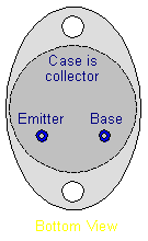
This is the pin out configuration of a TO-3 transistor. The test procedure is the same as the bipolar transistor in the next diagram. Take note of the pins labeled on the diagram for the TO-220 case transistor.
In this diagram, the volt meter applies a small voltage to the transistor's junctions. With the leads in this position, the junctions are forward biased. The reading should be between 0.5 and 0.7 volts. Readings outside this range are likely defective.
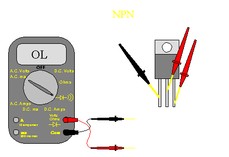
In this diagram, the junctions are being checked with reverse bias. No current should flow through the transistor's junctions with the leads in this position. The meter reading should be the same as it would read with open leads.
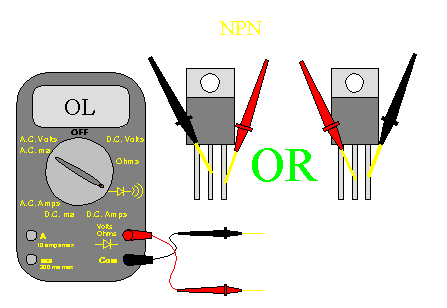
Both of these connections should also read as open. any other readings indicate defective transistors. The only exception will be with darlington transistors.
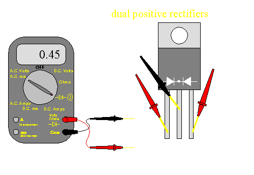
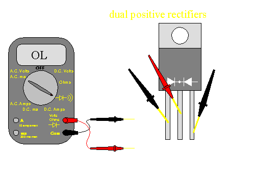
Checking Dual Diodes Now, I know that these aren't transistors but since we were checking things... :-) These first 2 diagram show how to check the dual positive rectifiers (diodes) and the associated meter readings. The windings of the transformer would go to the two outside legs and the center terminal would go to the positive rail capacitor.
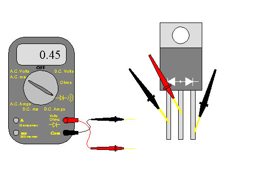
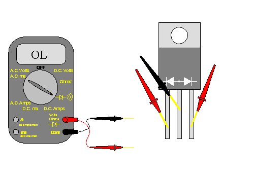
The next 2 diagram show how to check the dual negative rectifiers (diodes) and the associated meter readings. The windings of the transformer would go to the two outside legs and the center terminal would go to the negative rail capacitor.
If any combinations of meter leads to component terminals on any of the aforementioned devices reads less than 0.2 volts, the device is bad. Remember to test the FETs in the proper order. All of the devices must be removed from the circuit to obtain reliable test results. Some of the devices can be checked in circuit to see if they have any internal short circuits. There should be no connections on any of the devices that will cause the meter to read 0.00 while on diode check. The only exception will be the rectifiers. The outside legs of the dual rectifiers will be directly connected through the transformer windings and will appear to be a dead short. |
| If you find a problem
with this page or feel that some part of it needs
clarification, E-mail
me. This is a link to this site's home page. |